“Generating sustainable energy is not only crucial to mitigate global warming, but it is also important for geopolitical reasons to be independent of fossil fuels,” says Lukas Hrachowina, a researcher at NanoLund who recently defended his thesis, Growth and Characterization of Tandem-Junction Photovoltaic Nanowires.
He explains that conventional solar cells made of silicon are limited in efficiency:
“Because one material alone cannot convert the whole range of the solar spectrum into electricity without loss. The world record solar cells are based on multi-junctions that combine several so-called III-V semiconductors.”
Combining materials with nanowires
However, III-V semiconductors are expensive, and multi-junction solar cell films are not economically viable for terrestrial applications. The research group, led by Magnus Borgström, has combined these materials within nanowires. This has the potential to save about 90 percent of the semiconducting materials while retaining high efficiency.
“In times of global warming, it is important to discover new sustainable energy sources and to improve existing technologies. Nanowires can be used to fabricate solar cells that have high efficiency, are flexible, or semi-transparent. Nanowires are even interesting for space applications because they are radiation hard due to their geometry.”
This has the potential to save about 90 percent of the semiconducting materials while retaining high efficiency.
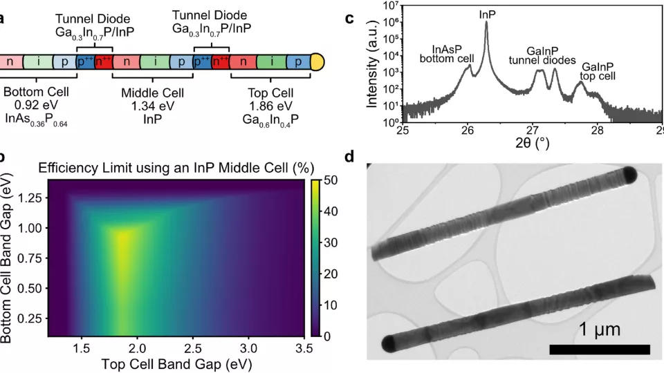
An essential part of a multi-junction solar cell is the Esaki tunnel diode that electrically connects the different materials.
“We found a convenient way to characterize our samples by measuring the electron-beam-induced current inside a scanning electron microscope. Once we learned how to combine one junction with the tunnel diode, it became feasible to add more junctions.”
By combining several junctions, the voltages of the subcells are added up. This made it possible to increase the power output and thereby the efficiency of the solar cell.
“However, the current of the solar cell is limited by the junction producing the least current. Therefore, it is important to carefully match the currents of all subcells – this will be the next step.
How can your results be useful?
“Our photovoltaic triple-junction nanowires show almost ideal addition of the open circuit voltage of the subcells and we have measured up to 2.37 V. The open-circuit voltage is twice as large as previously reported for tandem-junction photovoltaic nanowires and amounts to 94 percent of the sum of the respective single-junction nanowires. When fabricated into solar cells our photovoltaic triple-junction nanowires have the potential to reach a power conversion efficiency of up to 47 percent,” says Lukas Hrachowina.
Was there something in the results that took you by surprise?
Surprisingly, it was not trivial to just add the Esaki tunnel diode on top of the subcells. We found that a parasitic junction is formed but could circumvent this by introducing a charge selective barrier between the subcell and tunnel diode. This discovery was enabled and visualized by the electron-beam-induced current measurements.
(The Esaki tunnel diode constitutes the first quantum electron device. It is a type of semiconductor diode that has effectively “negative differential resistance” due to the quantum mechanical effect called tunneling. It was invented in 1957 and named after the Nobel Prize Laureate Leo Esaki.)
Read more about the illustration above – scroll to the second page!