Many in Europe have been eagerly awaiting the results of the first calls in the European Chips Act for pilot lines, with the aim is to enhance existing and develop new advanced pilot lines across the Union to enable development and deployment of cutting-edge semiconductor technologies and next-generation semiconductor technologies.
Also, we in NanoLund have our stake in the call, and have together with Swedish partners at Linköping, Chalmers and KTH been invited to be part of a pilot line for Wide Bandgap materials. We were very happy when the Chips JU announced that the Public Authorities Board approved all four pilot line proposals.For Lund University and LTH, the Faculty of Engineering this means an important piece in the puzzle of a strategic initiative within the semiconductor area.
Lund University and Vanya Darakchieva will lead the Workpackage on III- N radiofrequency and power device technologies of the Wide Bandgap pilotline and will contribute with a total effort of more the 8 M€ over 5 years.
“It is a great honour to be internationally recognized for our leading role in research on wide-bandgap materials for power electronics. We are happy and eager to work together with European partners and industries for establishing a resilient wide band gap semiconductors ecosystem” says Vanya Darakchieva.
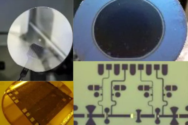
For the local research groups of Vanya Darakchieva and Erik Lind, as well as Lund Nano Lab, this means an influx of over 4 million euro, which must be backed with the same amount in national funding. The local contribution is based on the equipment available in Lund Nano Lab as well as expertise in III-Nitride and gallium oxide materials synthesis and characterization. The III-Nitride activities are focussed on the developments of state-of-the-art epitaxy, radiofrequency and power HEMTs and FinFETS. The target applications for power devices include smart grid, electric train traction, wind turbines, power components for propulsion and charging of electric vehicles. The III-nitrides rf electronic devices target power generation and amplification at high frequencies above 100 GHz for future wireless communication infrastructure, and for transmitters as well as rugged and linear receivers for surveillance and security systems.
Through the industrial collaboration within the Centre for III-nitride technology (C3NiT), a Vinnova Competence Centre also led by Vanya Darakchieva, the pathway to innovation where these technologies lead to an actual benefit in society is facilitated. It will also be an important development of Lund Nano Lab.
The EU Chips act is a key step for the EU’s technological sovereignty and an investment of close to 11 billion € in Europe’s competitiveness and resilience in semiconductor technologies and applications and help to achieve both the digital and green transition. In force since 13 September 2023, one of its first actions focussed on advanced pilot lines.
The proposal is coordinated by the Italian National Research Council (CNR) and includes partners from France, Poland, Finland, Germany, Austria and Sweden.