Materials & Manufacturing
The physical basis for nanomaterials research
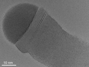
We aim to understand how nanomaterials form and how their properties emerge from their atomic and nanoscale structure. We explore both physical and chemical synthesis methods to generate nanostructured materials for fundamental research, future nanotechnology and industrial production.
On this page:
- Subareas within Materials & Manufacturing
- Publications
- Recent PhD-theses relevant to Materials & Manufacturing
- Key faculty in Materials & Manufacturing
Subareas within Materials & Manufacturing
- Compound semiconductors
Exploring new materials from a foundation in III-V semiconductors - Quantum materials and emergent phenomena
When the sum is larger than the parts - Novel nanofabrication
Novel nanofabrication methods, and integrating nano in industrial production.
Publications
2025
- Wahlqvist, D. Interaction and what follows: Electron beam effects in dynamic systems. Centre for Analysis and Synthesis, March 2025.
- Bermeo Vargas, M. Advancing Palladium-Based Nanostructures for Catalysis: From Nanoparticles to Multifunctional Nanoarchitectures. Solid State Physics, April 2025.
- Bjerke, A. Tool wear and tool protection in metal cutting: in-process interaction between workpiece, tool, and environment. Production and Materials Engineering, May 2025.
- Hu, T. In Situ Growth of GaP Nanowires with Alternative Seed Materials, Centre for Analysis and Synthesis, May 2025.
- Ternero, P. Ablating Boundaries, Sparking the Future of Materials: Engineering of Bimetallic Nanoparticles via Spark Ablation. Solid State Physics, May 2025.
- Sedrpooshan, M. From Nanoscale Design to Functional Integration of Magnetic Nanoparticle Assemblies: A Gas-Phase Strategy. Synchrotron Radiation Research, June 2025.
- Yadav, R. Low-dimensional Bismuth-induced structures on III-V semiconductor surfaces. Synchrotron Radiation Reserach, October 2025
2024
- Olausson, P. III-V Devices for Emerging Electronic Applications. Nano Electronics, January 2024.
- Athle, R. , Ferroelectric Memristors - Materials, Interfaces and Applications. Department of Electrical and Information Technology, March 2024.
- Bolano Losada, I. Modeling Photofunctional Transition Metal Complexes. Computational Chemistry, April 2024.
- Lindvall, R. Wear Mechanisms in Cutting Tools for Machining Applications : Interfacial Phenomena, Characterization, and Relation to Performance. Production and Materials Engeneering, May 2024.
- Wallander, H., Structure, oxidation, and catalytic activity of platinum-tin surfaces. Synchrotron Radiation Research, October 2024
- Alshemi, A. Tuning Interactions in Correlated Electron Systems: From Two-Band Superconductivity to Quasi-1D Spin Chains. Synchrotron Radiation Research, December 2024
2023
- Abbondanza, G. Ordered arrays of low-dimensional Au and Pd. Synchrotron Radiation Research, January 2023
- Hammarberg, S. Strain Mapping of Single Nanowires using Nano X-ray Diffraction. Synchrtron Radiation Research, January 2023
- Menon, H. Infrared Photodetectors based on InSb and InAs Nanostructures via Heterogeneous Integration-Rapid Melt Growth and Template Assisted Selective Epitaxy. Electrical and Information Technology, June 2023
- Benter, S. Adventures of III-V Semiconductor Surfaces. Synchrotron Radiation Research, October 2023
- Gilbert, J. Unravelling the structure and dynamics of lipid nanoparticles for biomolecule delivery. Physical Chemistry, October 2023
- Larsson, A. The Formation and Breakdown of Passive Film on Ni Alloys: in situ synchrotron studies. Synchrotron Radiation Research, December 2023
- Suchan, K. Life and Death of Mixed Metal Halide Perovskites: Mechanism and Consequences of Light Induced Halide Segregation in MAPb(I,Br)3. Chemical Physics, May 2023
- Snellman, M. Aerosol Synthesis and Characterization of Heterogeneous Bimetallic Nanoparticles. Solid State Physics, December 2023
- Franzén, S. Design and development of solid-state nanostructures for catalysis. Solid State Physics, December 2023
- Anders Gustafsson
- Anders Mikkelsen
- Arkady Yartsev
- Aylin Ahadi
- Dmitry Baranov
- Donatas Zigmantas
- Edvin Lundgren
- Elizabeth Blackburn
- Erik Lind
- Eva Unger
- Håkan Pettersson
- Ivan Maximov
- Ivan Scheblykin
- Jan Knudsen
- Jan-Eric Ståhl
- Jens Uhlig
- Jesper Wallentin
- Joachim Schnadt
- Jonas Johansson
- Jonas Ohlsson
- Karen Edler
- Kenneth Wärnmark
- Kimberly Thelander
- Knut Deppert
- Lars Montelius
- Lars Samuelson
- Lars-Erik Wernersson
- Lindsay Merte
- Magnus Borgström
- Maning Liu
- Maria Messing
- Maria Sandsten
- Martin Ek Rosén
- Martin Magnusson
- Matias Kagias
- Mats-Erik Pistol
- Mattias Borg
- Petter Persson
- Rainer Timm
- Rasmus Westerström
- Reine Wallenberg
- Sara Blomberg
- Sven Lidin
- Tönu Pullerits
- Vanya Darakchieva
- Volodymyr Bushlya
Topical meetings
Topic: Materials & Manufacturing
Date: Thursdays, approximately monthly
Time: 09:00–10:00
Place: k-space
Organizer: Martin Ek Rosén, Mattias Borg & Erik van Loon
Area coordinators
People in Materials & Manufacturing
People on the Materials & Manufacturing e-mailing list (PDF, opens in LU Box)
WISE: Wallenberg Initiative Material Science for Sustainability
The Wallenberg Initiative Materials Science for Sustainability (WISE) is the largest-ever investment in materials science in Sweden and will encompass major efforts at six of Sweden’s leading universities over the course of (at least) 10 years.