Semiconductor materials are used in electronic devices because of their unique electrical properties. III-V semiconductor materials consist of elements from the third and fifth columns of the periodic table. When a III-V semiconductor is heated above a specific temperature, the fifth column element will evaporate, leaving droplets of the third column material and even moving around on its surface. The droplets could be used as starting points for manufacturing nano-sized objects like quantum dots or other electronic devices.
Topping aluminium pattern with palladium
“Droplet dynamics is always fascinating and has been studied for decades. By simply heating up a few simple compound materials, you can get a very rich behaviour,” says Sandra Benter from the NanoLund Center for Nanoscience at Lund University.
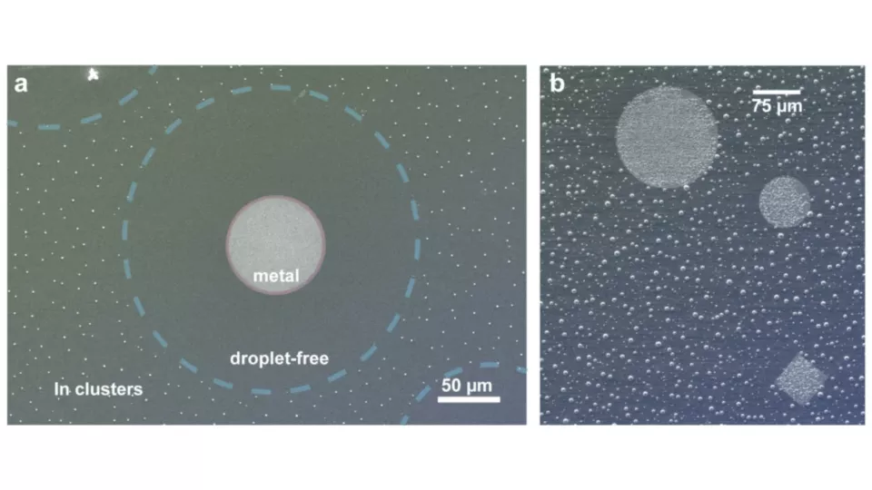
In the current study, the researchers printed a metal pattern of aluminium topped with palladium, resembling contacts like those commonly made for semiconductor devices, onto the surface before heating it. They found that the metal pattern inhibits droplets from forming in a zone around it under specific metal ratios and heating conditions. The result lets the researchers expand the temperature window without droplet formation and only form droplets where desired. The controllability leads to an increased toolbox of fabrication processes for on-chip devices.
We can locally tune the formation of nano and micron-sized droplets.
“The dramatic influence on droplet formation from these metal stacks was a surprise. We expected some effect, but this was rather much. We show that we can locally tune the formation of nano and micron-sized droplets,” says Sandra Benter.
The results of the study have implications for semiconductor electronics manufacturing.
Relevant far beyond
“It will be relevant for quantum computing, optoelectronics and various neuromorphic (Editors note: computer systems modelled from the human brain) applications where different mixed materials must be combined to create advanced systems. Also, we theoretically model the observed behaviour of the experiments and show that they are based on a few general assumptions found in many material systems, indicating that the ideas and results are relevant far beyond the system and process we chose,” concludes Sandra Benter.