Visitor Programs
The goal of outreach activities is to spread information about nanoscience and nanotechnology, including safety and sustainability aspects and opportunities to address important needs in society.
This can be lab tours, lectures, but also practical exercises.
Lab tours and lectures
School classes or student groups that are interested to make an appointment for a tour are invited to contact our outreach coordinator, Adam Burke.
E-mail: Adam [dot] Burke [at] ftf [dot] lth [dot] se (Adam[dot]Burke[at]ftf[dot]lth[dot]se)
Demonstration how to work with scanning electron microscopy - Spherical Image - RICOH THETA
Demonstration how to work with scanning electron microscopy for a group of visitors – Spherical Image
NanoLund is part of the Lund University NMT days, that are organized each year in March for high school students and teachers. NMT stands for “Natural Sciences, Medicine and Technology” and comprises more than 100 lectures at a popular scientific level.
Schedule and registration for NMT days 2021 (page in Swedish)
Meet us outside the lab
We visit you
We are very happy to visit schools or organizations to give lectures or shorter demos. Currently, we can offer the following:
- One hour introductory lecture at basic level: What is nanotechnology? (available both in Swedish and English)
- Lecture about advanced microscopy
- One hour lecture about nanosafety
- Demonstration experiment with a table-top Scanning Electron Microscope
2 Weeks Summer Visit
We are cooperating with Forskningsnätet, a non-profit organization dedicated to facilitating information flow from research to schools.
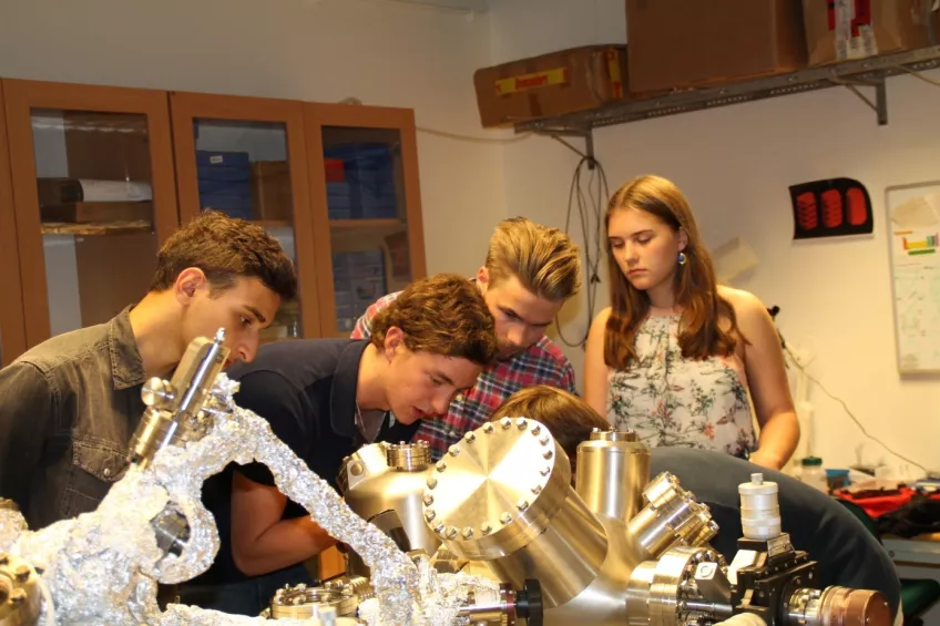
Each year, during two weeks of the summer holidays, a group of high school pupils nominated by Forskningsnätet, comes to us where our doctoral students and researchers take turns to introduce the pupils to certain aspects of nanotechnology research.
Demonstration of Scanning tunnel Microscopy for high-school students
For example, the lectures and practical exercises can cover the following topics:
- Laboratory Safety and specifics of working in a semiconductor nanofabrication cleanroom laboratory
- Introduction to microfluidics
- Microfabrication of devices for deterministic lateral displacement (DLD) and dielectrophoresis (DEP)
- Sorting of micro-and nanoparticles by DLD and DEP
- Electron Beam Lithography (EBL)
- Scanning electron microscopy (SEM)
- Fluorescence microscopy
- Chemical beam epitaxy (CBE)
- Scanning tunnel microscopy on Au(111) surface
- Theory of light absorption
- Aerosol nanoparticles and characterization
- Transmission electron microscopy (TEM)
- Low-temperature measurements
- Physics at the nanoscale (theory)
The topics vary each year, depending on what is at the forefront of nanoscience just then.
See the website of our outreach partner Forskningsnätet
Just curious?
In case you are just curious and would like to learn more about nanotechnology, please have a look at the popular scientific topics (Mission is possible articles)
Would you like to know more?
Please contact adam [dot] burke [at] ftf [dot] lth [dot] se (Adam Burke), Outreach coordinator.
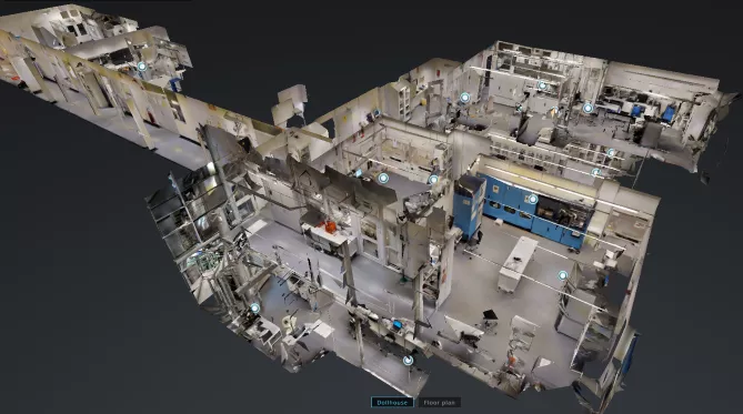
3D tour of Lund Nano Lab
Try our interactive tour of the clean room facilities to see where the research happens. Welcome in!
Video: 3D tour of Lund Nano Lab (1:00 minutes)
Video: 3D tour of Lund Nano Lab (4:00 minutes)
Inspiration for educators

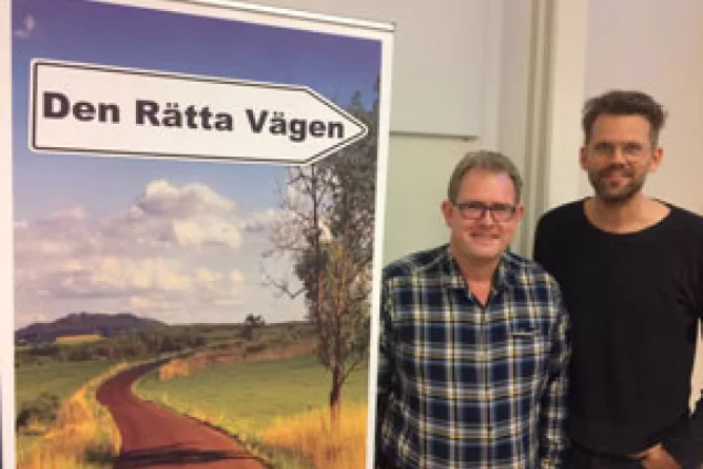
Theatre on Nanoplastics
For schools: theatre and workshop (link to Swedish site)


