Exploratory Nanotechnology
Exploratory Nanotechnology is the testing ground for innovative nanotechnology concepts, to evaluate their strategic importance for NanoLund. We explore novel top-down methods to fabricate nanostructures and devices, as well as utilizing self-assembly approaches, with the aim to realize atomic level control. We investigate possible ways to combine heterogeneous materials and devices in three dimensions, as well as exploring novel material properties emerging due to the nanostructuring and long-range order of materials.
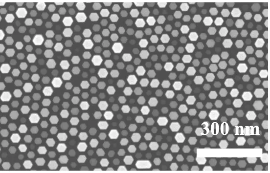
Scanning Electron Microscopy top view of InAs vertical nanowires grown InAs/Si substrate by a selective area epitaxy with SiNx as a mask. The silicon nitride mask was patterned by a Block-Copolymer (BCP) lithography using hexagonally-oriented, vertical cylinders formed in a 50 nm pitch PS-b-P4VP polymer system. Photo: Anette Löfstrand
Atomic Sculpting
Patterning methods at the nanoscale play a decisive role in our capability to make nanostructures with good control of their interfaces and thus electrical, optical and other properties of the devices. What approaches can be used to achieve highest possible resolution, preferably with atomic-scale accuracy with high throughput? This and other questions are addressed in Novel patterning methods, which include new lithography and etching approaches.
Enabling technology for 3D Heterointegration
The combination of materials and devices that traditionally do not go together can open a wide range of scientific and technical opportunities. Here we explore new processes and technology to combine advanced materials of high quality that can enable new physics and breakthroughs in system performance. We focus specifically on methods to integrate distinct materials and functionality on top of each other (3D) without degradation of underlying structures.


