Enabling technology for 3D Heterointegration
The combination of materials and devices that traditionally do not go together can open a wide range of scientific and technical opportunities. Here we explore new processes and technology to combine advanced materials of high quality that can enable new physics and breakthroughs in system performance. We focus specifically on methods to integrate distinct materials and functionality on top of each other (3D) without degradation of underlying structures.
Project areas:
Low thermal budget III-V integration with CMOS
The III-V semiconductors have many properties, such as small effective mass and direct and tunable band gaps, that would enhance existing Si CMOS technology, could the materials be monolithically integrated at a low enough thermal budget so as not to damage the Si front-end. A main challenge to this aim is the severe defects formed at the junction between Si and the III-V crystals. By minimizing the size of this interface, the negative effects of these defects can be minimized. We explore CMOS-compatible novel methods to integrate III-V micro- and nanostructures with Si. This includes direct growth of III-V nanostructures within hollow oxide templates and rapid melting and recrystallization. By limiting the heating in time and spatial extent by flash-lamp and pulsed laser annealing we aim to achieve high quality III-V semiconductor devices that can be placed on top of Si CMOS devices.
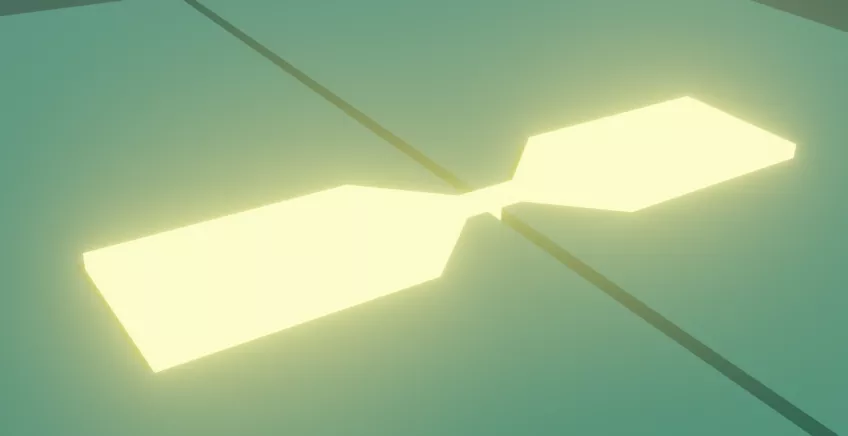
Illustration of a III-V melt inside a dielectric micro-crucible, with only a nanoscale contact point with the Si substrate.
III-V integration with 2D materials
The so-called 2D materials (graphene, hexagonal boron nitride, MoS2, WSe2 etc.) are highly interesting by themselves, but here we explore their combination with III-V semiconductors. The electronic transport across the 2D to 3D/1D junction via van der Waals bonding can provide exciting physical phenomena which may be harnessed in electronic devices. We explore III-V epitaxy on top of 2D material substrates with the aim of creating a platform for enabling high-performing InAs electronic devices on amorphous substrates.
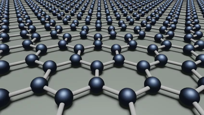
Illustration of graphene monolayer on a substrate. Graphics: Mattias Borg
Nanowire film transfer
One way to integrate nanowire devices with other technologies is to transfer the nanowires post-growth onto an already processed chip to add functionality. One such application is to add a nanowire solar cell in parallel with a Si solar cell to improve the coverage of the solar spectrum. This can be accomplished by encasing a forest of nanowire p-n junctions, with a suitable band gap and grown on a native III-V substrate, in a polymer film and lifting off the entire film and nanowires and transferring the nanowires still standing onto another substrate. Here we focus on the development of this transfer technique to maximize the yield of transferred nanowires, reproducibility of the process and reusability of the source substrate.
Key publications
Facet-selective group-III incorporation in InGaAs template assisted selective epitaxy. Borg, M, Gignac, L, Bruley, J, Malmgren, A, Sant, S, Convertino, C, Rossell, MD, Sousa, M, Breslin, C, Riel, H, Moselund, KE & Schmid, H. Nanotechnology, vol. 30, no. 8 (2019), 084004. DOI: 10.1088/1361-6528/aaf547
See article facet-selective group-III incorporation at publisher's site
Au-Seeded Growth of Vertical and in-Plane III–V Nanowires on Graphite Substrates. Wallentin, J, Kriegner, D., Stangl, J., Borgström, M., Nano Lett. 2014, 14, 4, 1707-1713. DOI: 10.1021/nl403411w
See article Au-seeded growth at publisher's site